

Product Name : IC Design Application
Description
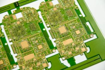
 Technologies
●Any layer HDI
●Aspect ratio up to 25
●Back drill
●Board thickness 10 mm / 390 mil
●Cavity down
●High speed and low loss materials
●Layer count up to 40
●Micro via copper-fill plate
●Minimum line width / spacing 2 mil (50 micro meters)
●Thermal management-coin inserted
●VIP (via in pad) :
conductive-conductive copper paste ;
non-conductive-epoxy via hole fill
Applications
Smart Phones, Internet of Things, Multimedia A/V, Telecommunication Equipment, Sensing Component, Smart TV, DVD/Blu-ray Storage System, Smart Audio System, Home Networking Device System, Smart CPU&GPU, Broadband Gateway and Set-top Box, Tablet, LTE Modem Platform, RF Transceiver, NFC( Near Field Communication) Product, Bluetooth Product, GPS (Global Positioning System) Product, Wireless Charging and Wearable Device.
conductive-conductive copper paste ;
non-conductive-epoxy via hole fill