PCB Advanced Technology
Nowadays, PCBs is needed for transmit high-frequency signals at high speeds, lower signal loss. According to above, signal integrity and thermal management are more important. Shin Puu continuously develops advanced PCB capabilities and offer even next generation PCB technologies by strict quality management to help customer fulfill design functionality. Besides PCB / PCBA production, we set up a sourcing team who is with abundant experience and reliable connections with top material suppliers specific to each market. We are providing not just low cost, fast sourcing service but also smart substitution suggestions for customer consideration to optimize customer benefits on component procurement.
Our major key technologies including:
Our major key technologies including:
Advanced Technology of Shin Puu
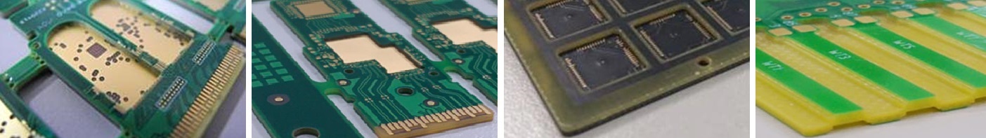
 High Speed Digital and RF/Microwave PCB
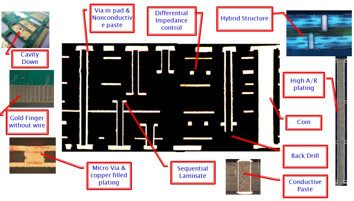
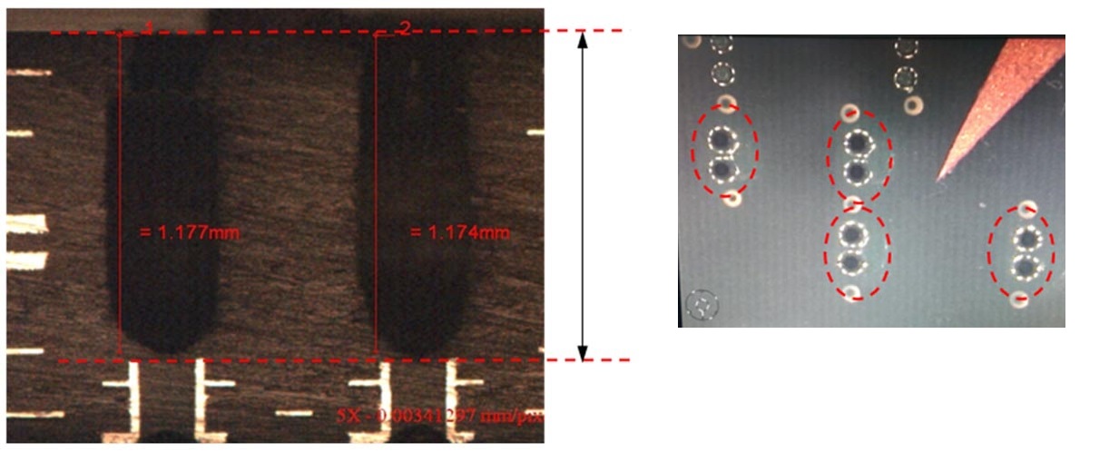
 ●Back Drill:
Back drilling of PCBs helps to remove signal distortion by removing via hole wall copper. It is a process to remove the unused section of plated through holes.
Back drilling of PCBs helps to remove signal distortion by removing via hole wall copper. It is a process to remove the unused section of plated through holes.
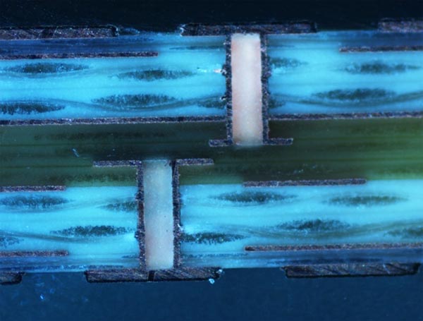
●Cavity Down:
Besides keeping mechanical design in a low profile format, cavity down can be used to reduce total thickness when inserted components or design for wave guide to reduce signal loss and raise speed of transmission for high-frequency signals, then limiting signal transmission in the slot at the same time.
Besides keeping mechanical design in a low profile format, cavity down can be used to reduce total thickness when inserted components or design for wave guide to reduce signal loss and raise speed of transmission for high-frequency signals, then limiting signal transmission in the slot at the same time.
●Hybrid or Composite Construction:
It can be designed by laminating microwave materials ( ex. Rogers ACS products) with high-speed FR-4 materials to achieve the purposes of high-speed, high-frequency and cost effective solutions.
It can be designed by laminating microwave materials ( ex. Rogers ACS products) with high-speed FR-4 materials to achieve the purposes of high-speed, high-frequency and cost effective solutions.
●Strict Impedance Control Capability:
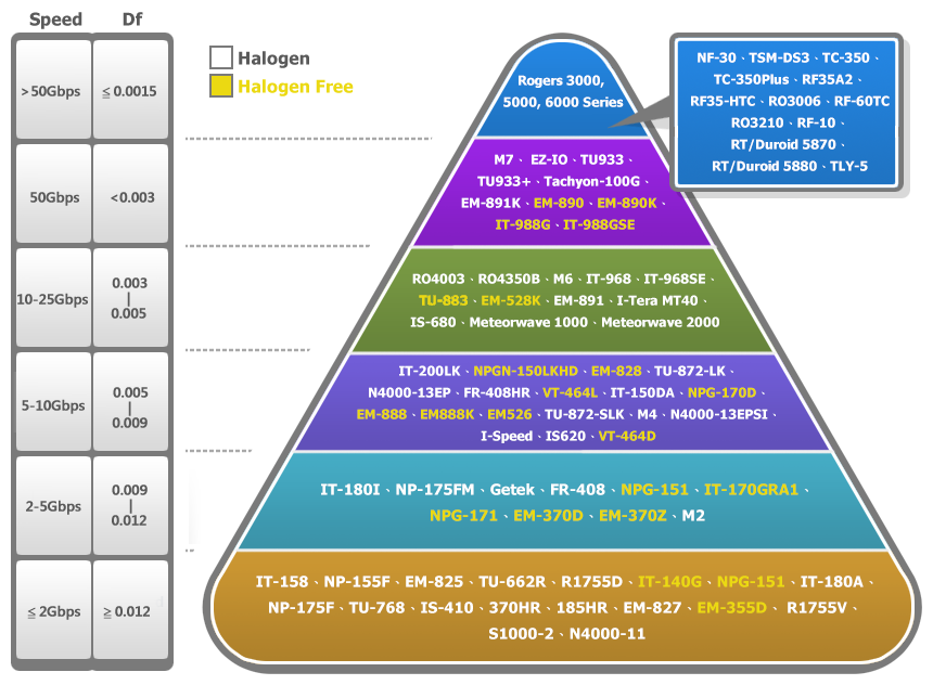
Shin Puu can provide design recommendations for impedance design and has many experiences in high-speed and RF/microwave PCB manufacturing. Our engineers will adjust the line width, copper thickness, stacking, etc. base on Dielectric Constant (Dk) and Dissipation Factors(Df) of material by actual manufacturing experience according to the customers' required design and impedance specifications.
Shin Puu can provide design recommendations for impedance design and has many experiences in high-speed and RF/microwave PCB manufacturing. Our engineers will adjust the line width, copper thickness, stacking, etc. base on Dielectric Constant (Dk) and Dissipation Factors(Df) of material by actual manufacturing experience according to the customers' required design and impedance specifications.
Thermal Management
●Coin Insertion Technology:
It embeds a piece of metal coin inside PCB under the high power components, so the heat created from the components can be effectively dissipated through the coin to another side of the PCB. Since the coin is small and light weight, it has great advantage of lower cost and very good performance. This technology has been used in the PCB of base stations, point-to-point radio and military radar systems. It is also under testing for IC substrate application now.
It embeds a piece of metal coin inside PCB under the high power components, so the heat created from the components can be effectively dissipated through the coin to another side of the PCB. Since the coin is small and light weight, it has great advantage of lower cost and very good performance. This technology has been used in the PCB of base stations, point-to-point radio and military radar systems. It is also under testing for IC substrate application now.
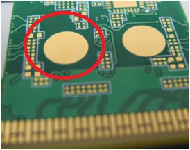
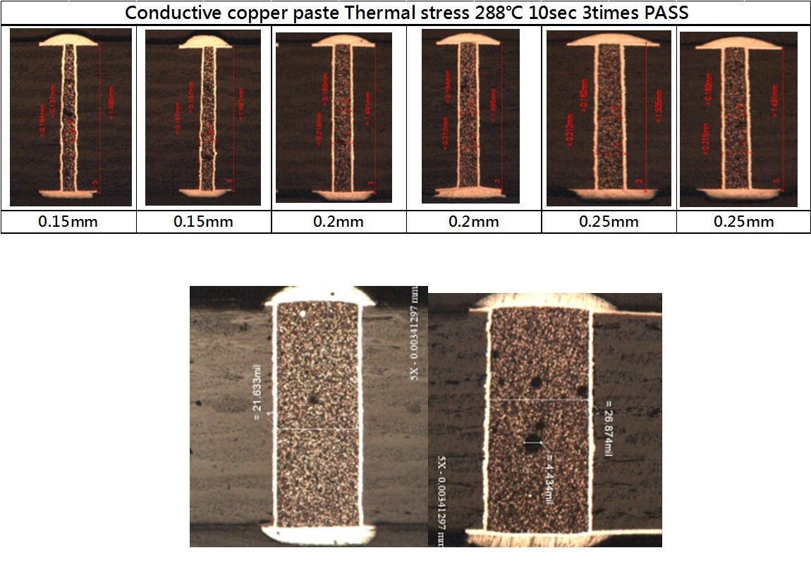
●Conductive Copper Paste:
Similar to the copper insertion technology, the conductive copper paste is used to fill the hole for heat dissipation. We adopted Tatsuta solutions, please refer to below website for more information:
http://www.tatsuta.com/products/functional-material/paste/.
Similar to the copper insertion technology, the conductive copper paste is used to fill the hole for heat dissipation. We adopted Tatsuta solutions, please refer to below website for more information:
http://www.tatsuta.com/products/functional-material/paste/.
Various Special Materials in Use Shin Puu has extensive experience in PCB manufacturing and uses a variety of special materials. Therefore, we can assist customers in selecting the most appropriate and cost-effective material.
For more information of material, please refer to "PCB Material We Use".