

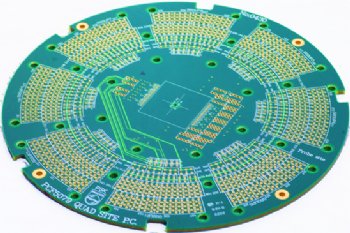
Product Name : Semiconductor Testing and Testing Equipments
Description
 Technologies
●Aspect ratio up to 25
●Big size board assembly
●Board flatness <0.3%
●Board thickness 9.1 mm
●Embedded component PCB
●High speed and low loss materials
●Layer count up to 40
●Minimum line width / spacing 2 mil
●VIP (via in pad) :
conductive-conductive copper paste ;
non-conductive-epoxy via hole fill
Applications
Burn-in, load board and probe Card
conductive-conductive copper paste ;
non-conductive-epoxy via hole fill